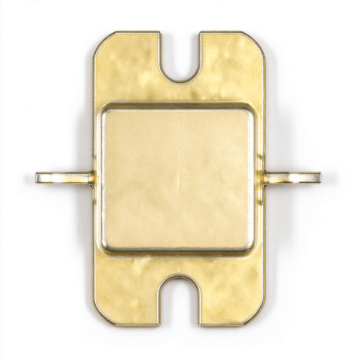

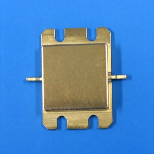
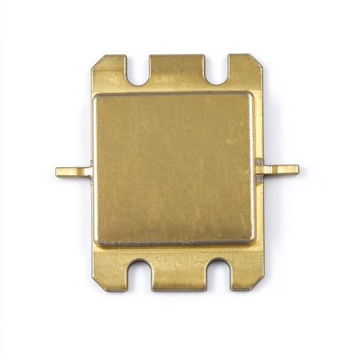
IMPA008020P40 GaN Power Transistor
Technical Highlights
0.8–2.0GHz Ultra-Wideband Coverage
The IMPA008020P40 is an internally matched GaN HEMT power transistor with a specified operating band from 0.8GHz to 2.0GHz.
At Least 40dBm Saturated Output
The device delivers a minimum saturated output power of 40dBm under the specified +28V CW test conditions.
Broadband Gain and Efficiency
Specified minimum performance includes 11dB power gain and 41% power-added efficiency across the rated band.
50Ω Internally Matched RF Interfaces
The internally matched input and output simplify integration into broadband communications and radar RF power stages.
Electrical Specifications
| Device Technology | GaN HEMT |
|---|---|
| Specified Frequency Range | 0.8–2.0GHz |
| Characterization Coverage | The supplied measurement table additionally includes data from 0.5GHz to 0.7GHz; these points are outside the stated operating band. |
| Saturated Output Power | 40dBm minimum |
| Power Gain | 11dB minimum |
| Power-Added Efficiency | 41% minimum |
| Power Flatness | 2dB maximum |
| RF Impedance | 50Ω input and output system |
| Primary Characterization Conditions | TA = +25°C, VDS = +28V, IDS = 30mA, CW |
| Quiescent Current Note | The electrical-specification condition block also lists IDsq = 50mA. Confirm the required bias condition before final design validation. |
| Pinch-Off Voltage | -8V to -4V at VDS = 6V and IDS ≤ 100mA |
| Gate-Source Reverse Current | 5µA maximum at VDS = 0V and VGS = -10V |
Package and Operating Limits
| Package Type | Hermetic metal-ceramic flanged package |
|---|---|
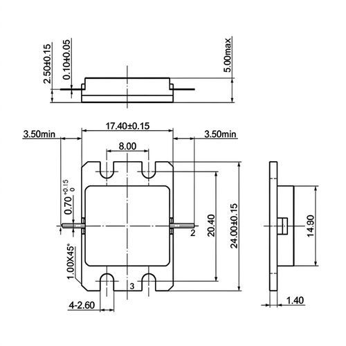
| Dimensions | 17.40 × 24.00 × 5.00mm maximum |
| Operating Temperature | -40°C to +85°C |
| Storage Temperature | -55°C to +125°C |
| Maximum Drain-Source Voltage | +120V |
| Maximum Gate-Source Voltage | -10V |
| Power Dissipation | 13W at TC = +25°C |
| Terminal Identification | Chamfered side: gate; flat side: drain |
Integration and Bias Notes
Apply the negative gate bias before applying the positive drain voltage.
During power-down, remove the drain voltage before removing the gate bias.
Use M2.0 mounting screws with a recommended tightening torque of 0.6N·m.
Provide a mounting slot width of at least 17.65mm and maintain a minimum 0.1mm lead-to-PCB height.
Keep the package temperature at or below +85°C during operation.
The reference circuit uses RO4350B material with 0.762mm thickness and a dielectric constant of 3.48.
The device is electrostatic-discharge sensitive; use grounded handling and assembly equipment.
FAQ
What is the specified frequency range of the IMPA008020P40?
The specified operating range is 0.8GHz to 2.0GHz. The supplied characterization table also contains measurements from 0.5GHz to 0.7GHz, but those points are outside the stated operating band.
What output power does the device provide?
The datasheet specifies a minimum saturated output power of 40dBm under the stated +28V CW test conditions.
What are the minimum gain and efficiency ratings?
The specified minimum power gain is 11dB and the minimum power-added efficiency is 41%.
Which quiescent current should be used?
The characterization page lists IDS = 30mA, while the electrical-specification condition block contains IDsq = 50mA. The required bias point should be confirmed before final design validation.
Does the device support CW operation?
Yes. The principal electrical performance table is specified under CW test conditions.
B2B Procurement FAQ
What information should be included in an inquiry?
Please provide the model number, requested quantity, operating band, intended application, destination country and required documentation.
Can evaluation quantities be requested?
Sample availability, quantity and lead time should be confirmed during quotation.
Is application-circuit information available?
Yes. The supplied documentation includes a recommended broadband application circuit using RO4350B RF laminate.
Can the bias-current discrepancy be clarified before ordering?
Yes. Buyers should identify the intended operating conditions in the RFQ and request written confirmation of the applicable quiescent-current setting.
Are lead time and minimum order quantity guaranteed?
No fixed commitment is stated in the supplied product material. Lead time, minimum order quantity and commercial terms should be confirmed for each quotation.